
Overview
The research undertaken by our lab is supported by extensive physics and engineering facilities, complemented by the skill sets of group members. These in-lab resources support computationally-intensive simulation studies of novel forms of x-ray converters and pixel circuits. The resources also facilitate creation of the complex, full-custom, hardware and software systems required to characterize the performance of converter and backplane prototypes. This has allowed design, fabrication and debugging of the electrical, mechanical and software sub-systems of a series of increasingly more capable (and more complex) electronic data acquisition systems – most recently the G4 system which allows performance characterization of active matrix flat-panel imager (AMFPI), active pixel and single photon counting array prototypes that are the basis of our research. Brief descriptions of selected facilities and resources in our lab are given below.

Computer Simulation
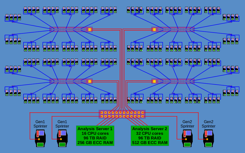
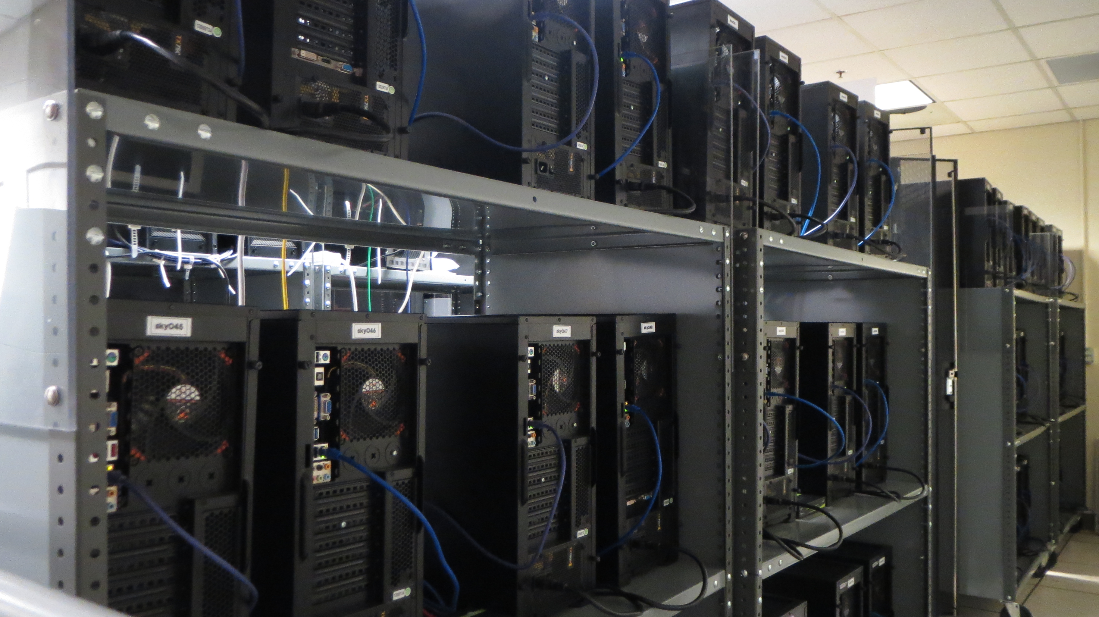
The research of our lab includes computationally intensive tasks – such as Monte Carlo -based simulations of radiation and optical transport in x-ray converters using EGSnrc and GEANT, as well as simulations of the operation of the backplane circuits of active pixel and photon-counting pixels using SPICE. To support this need, we have designed and built a laboratory computer cluster which includes a full-custom supercomputer. The cluster consists of 1536 cores across 192 parallel nodes offering ~25 TFLOPS, which provide the computing muscle to perform various tasks including radiation transport, optical transport, and circuit simulations. Two large memory servers (256 GB and 512 GB) provide enough RAM to efficiently transform data without waiting for storage IO. Multiple networked storage servers provide 100's of TB of resilient ZFS-backed storage capacity for easy access. Five sprinter nodes provide maximum single-threaded performance for tasks such as FPGA synthesis and data analysis. Our latest sprinter node runs at 5.1 GHz and includes 1TB of fast local NVMe storage. The network has a 24-port 10-Gbit Ethernet primary switch directly connected to the servers and to six 48-port secondary switches.
Mechanical Assembly Development
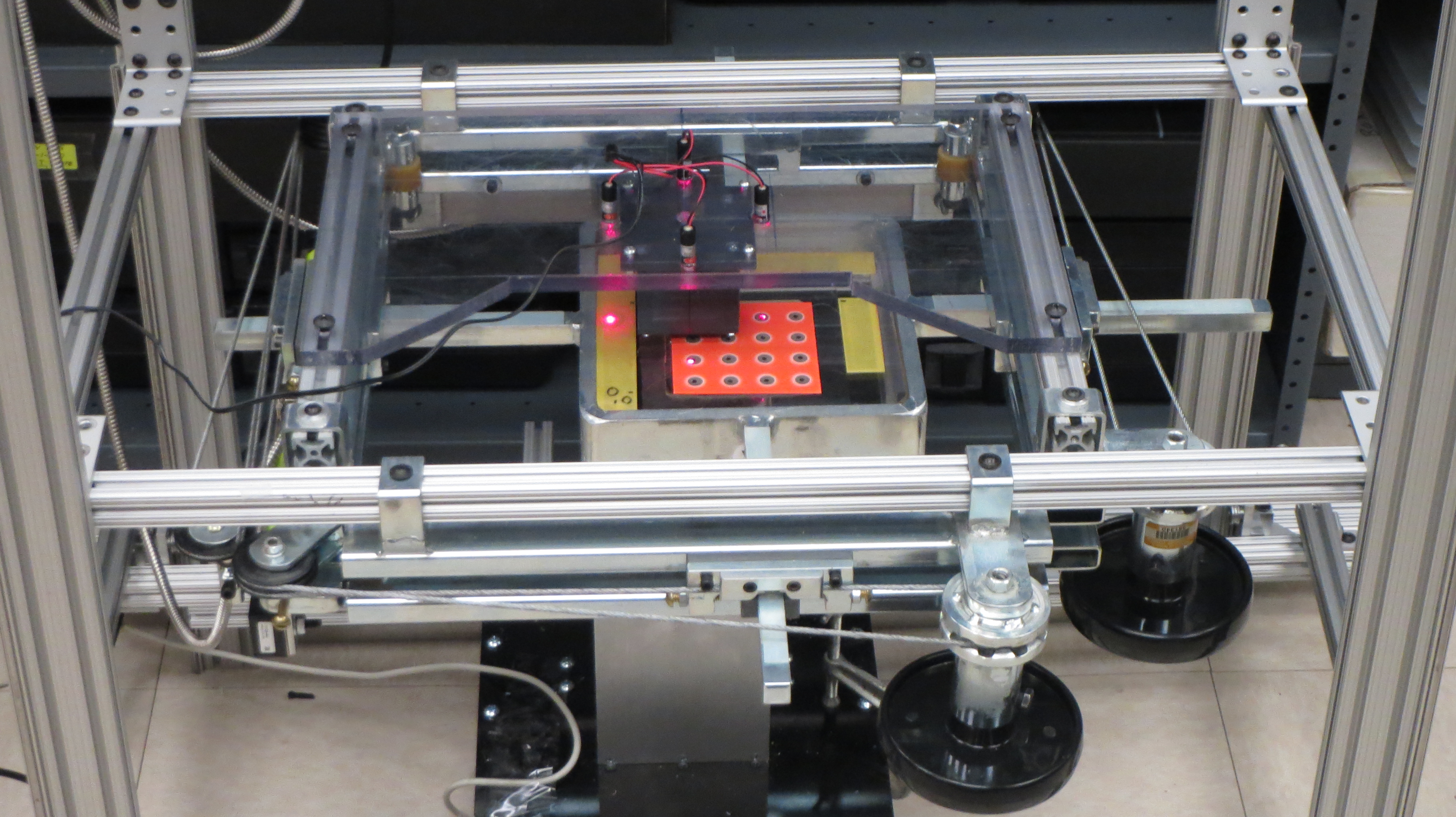
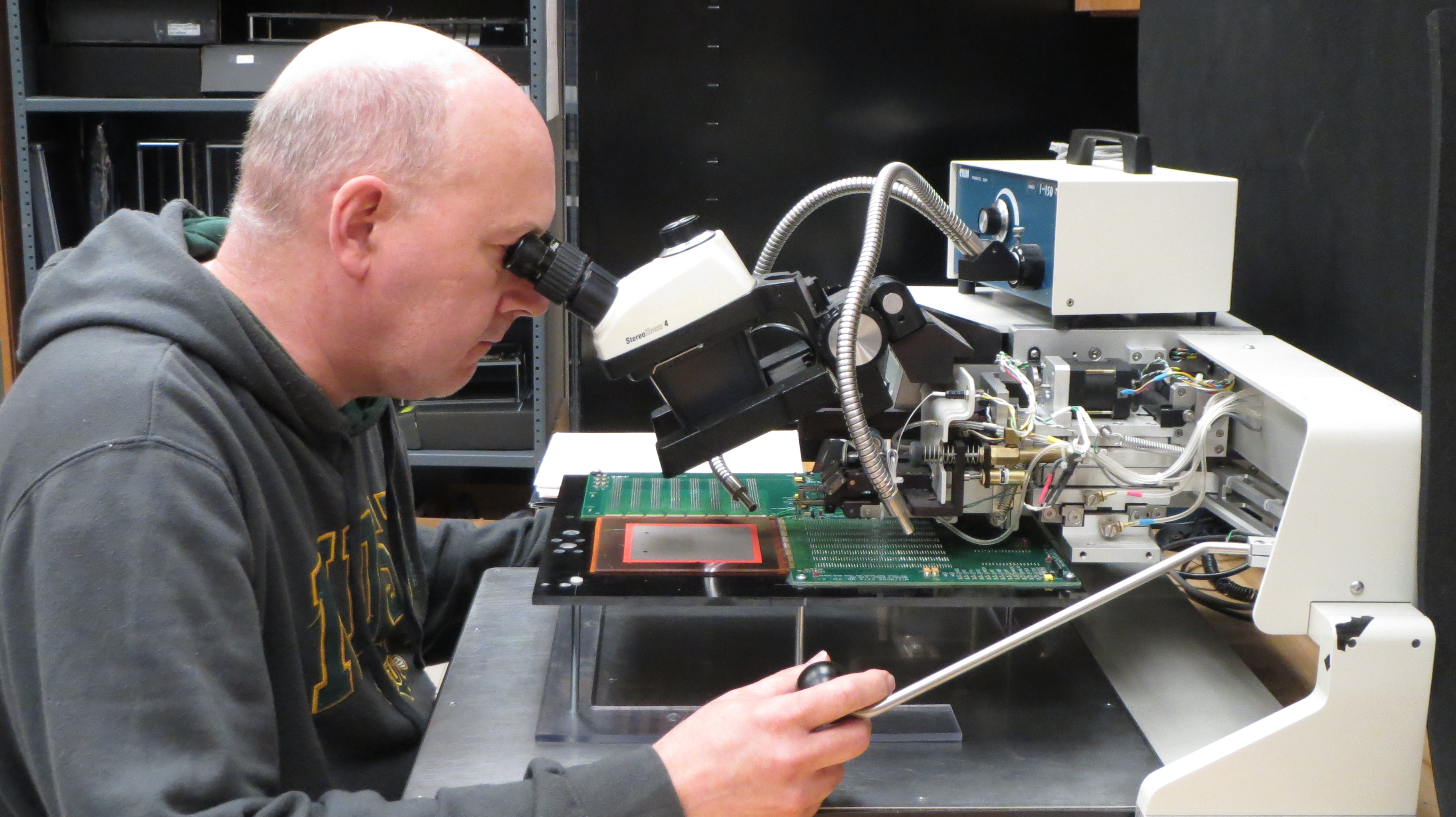
In order to conduct the research, our lab builds a wide variety of mechanical assemblages. One example (shown in the adjacent image) is a custom-designed positioning system for performing measurements of the material composition of photoconductors deposited on AMFPI arrays. Another example (in the accompanying image) shows a wire-bonding machine being used to establish electrical connections between an AMFPI array and peripheral data acquisition electronics.
Electronic Acquisition System Development
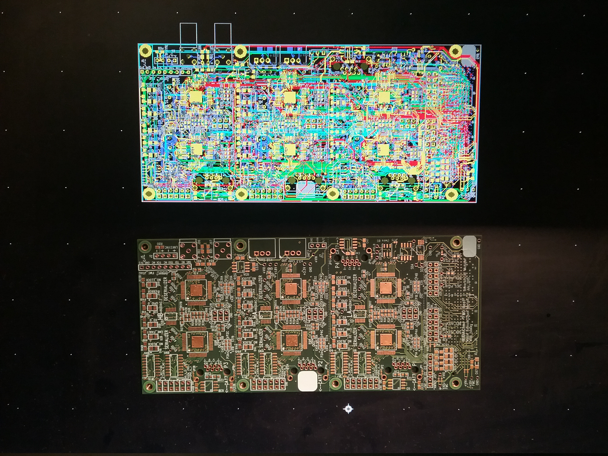
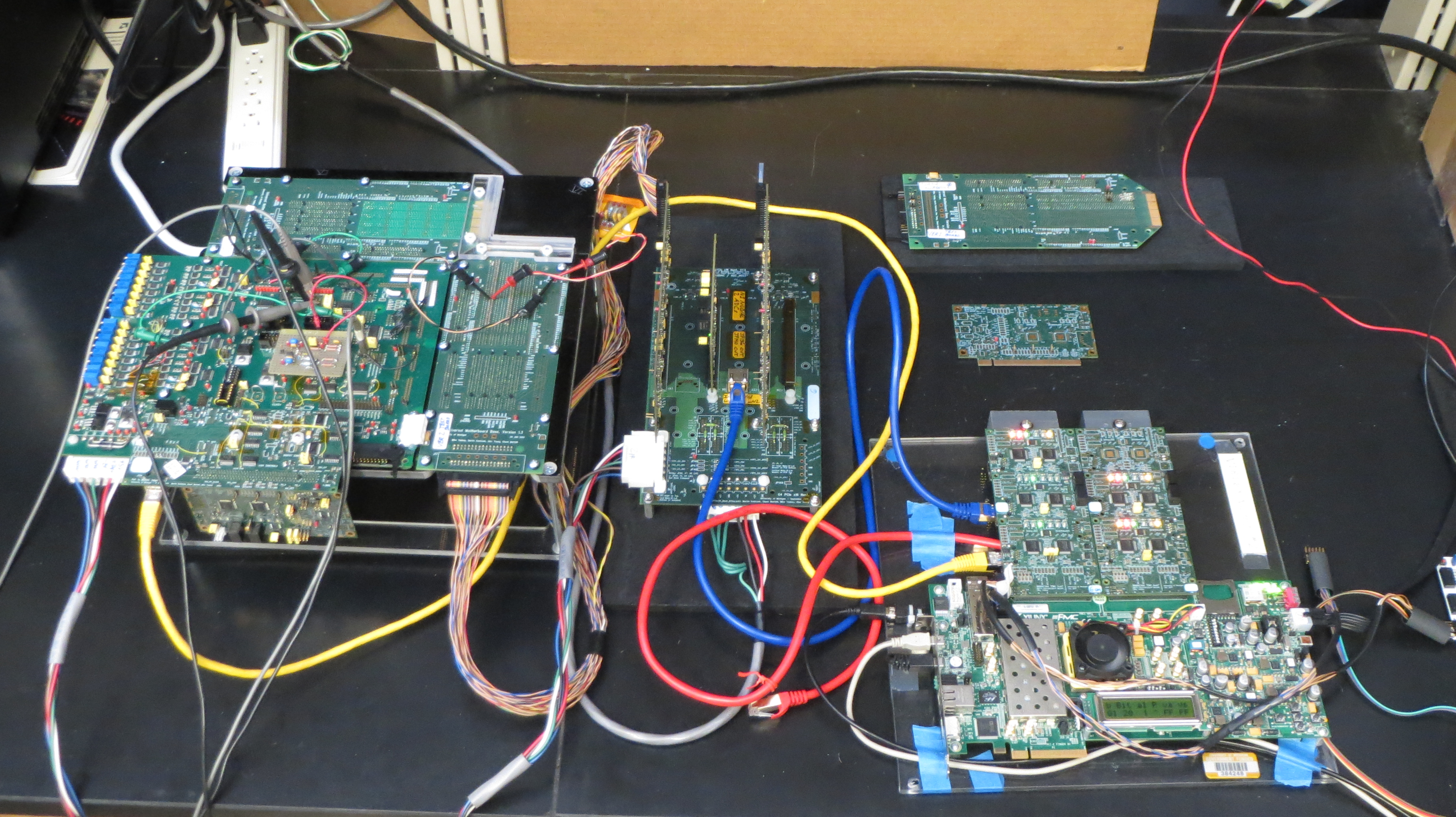
In order to carry out empirical characterizations of the various prototypes developed by our group, our lab designs, fabricates and debugs the various sub-systems of the electronic data acquisition systems required for the research. The adjacent image shows a rendering of a real-time communications board (top) along with the corresponding, manufactured printed circuit board. The accompanying image shows the digital heart of the G4 data acquisition system.
Measurement Station
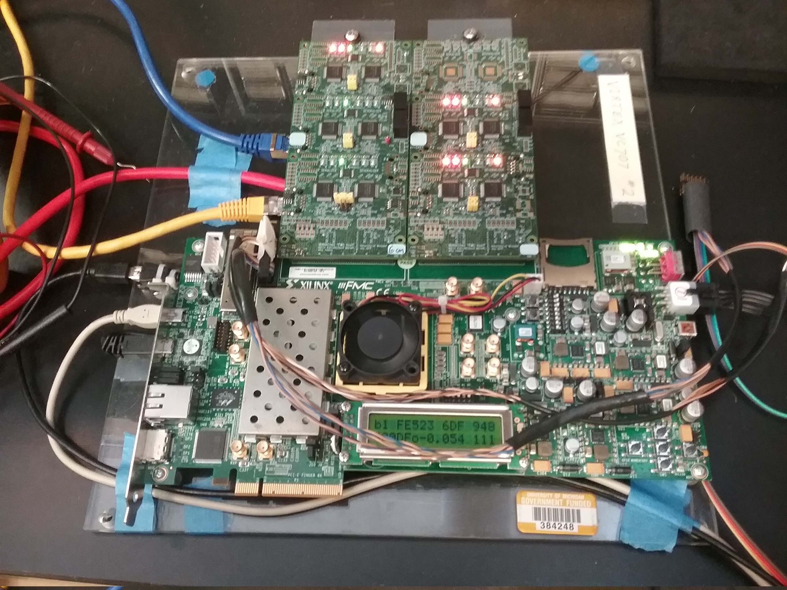
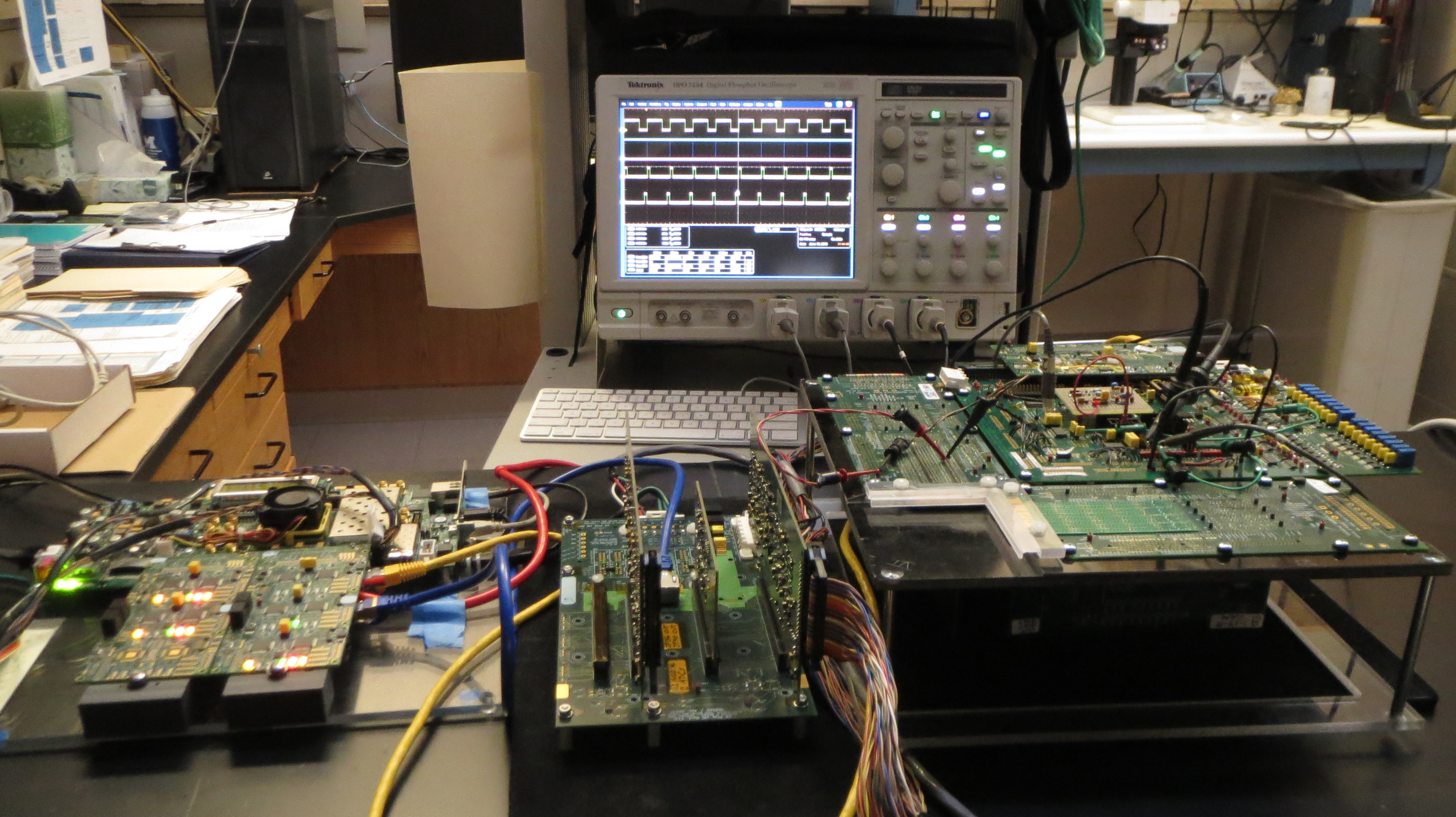
Our lab includes equipment for testing and operating AMFPI, active pixel and photon counting arrays as well as for measuring their performance under various conditions and stimuli. The adjacent image includes the front-end electronics of the G4 system that directly connects to an array, while the accompanying image shows those electronics connected to an oscilloscope configured to depict some of the control signals used to operate the array.
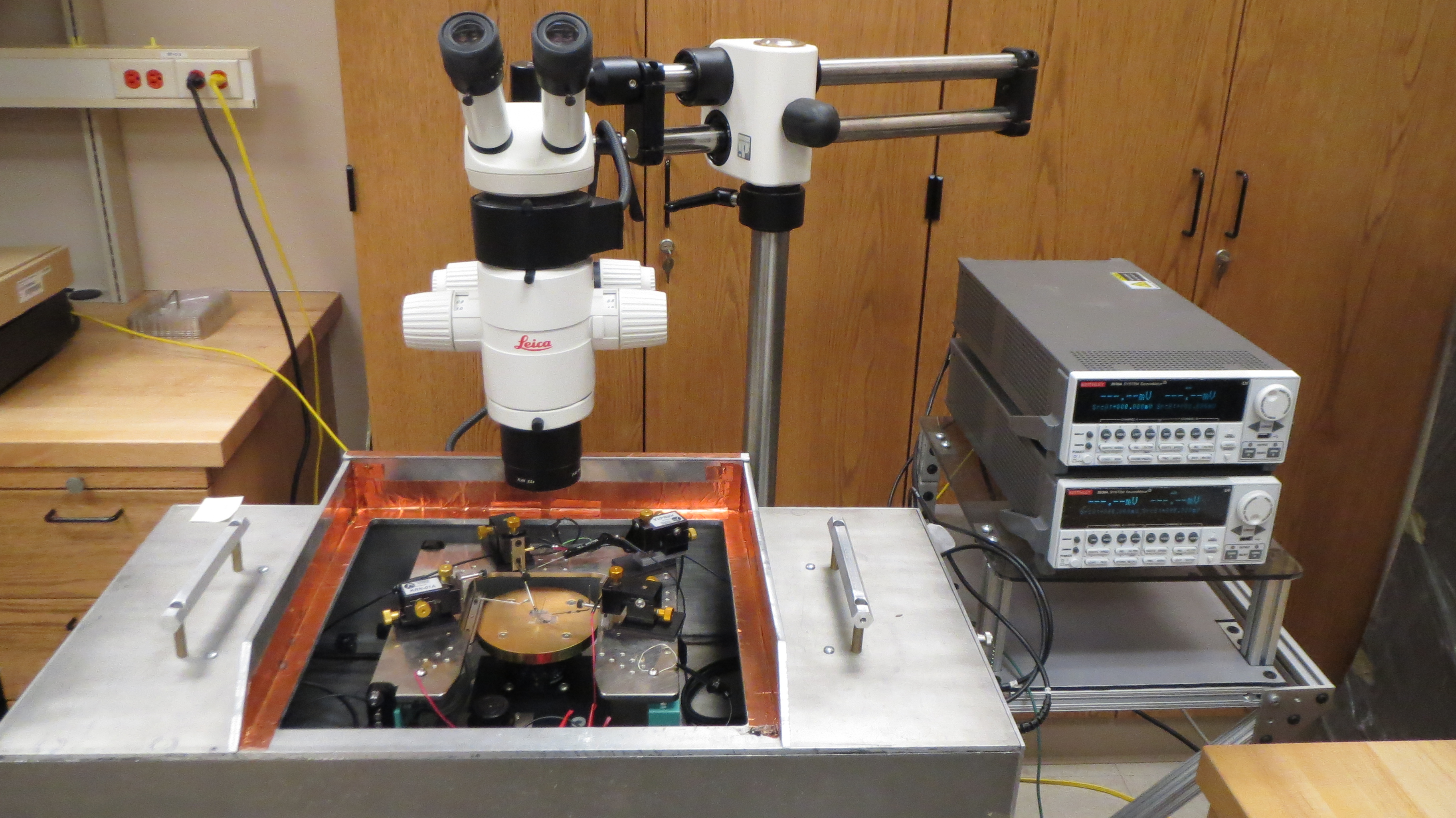
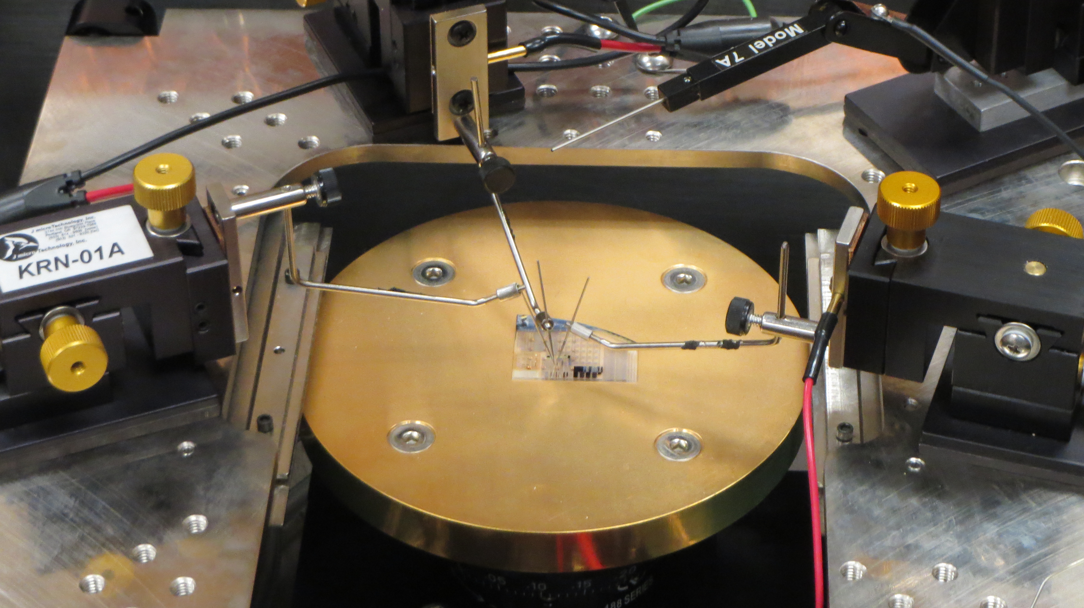
TFT Characterization
Our lab has constructed various probe stations for characterization of thin-film transistors (TFTs) fabricated from semiconductor materials of interest (e.g., polycrystalline silicon). The adjacent images show fine-tip probes connected to a TFT inside a metal electrical isolation box. A microscope is used to accurately position the probe tips on electrical contacts of the TFTs. To the right of this setup are a pair of source meter units, which are used to both operate and measure the TFTs.
Publications
Maolinbay et al., Nucl. Instr. Meth. A485(3), 661-675, 2002
Yarema et al., Nucl. Instr. Meth. A439(2,3), 413-417, 2000.
Huang et al., Nucl. Instr. Meth. A431, 273-284, 1999.
Morton et al., IEEE Trans. Nucl. Sc. 41(4), 1150-1154, 1994.
Morton et al., IEEE NNS Trans. 40(4), 1031-1035, 1993.